Contents
Overview
The concept of a 'process node' emerged from the need to standardize and market advancements in semiconductor fabrication. Early integrated circuits in the 1970s were measured in micrometers (µm). By the 1990s, the industry began transitioning to nanometer (nm) designations, a move that was initially tied to the gate length of the MOSFET transistor. Companies like Intel were pioneers. The journey from early micron-scale nodes to today's sub-10nm processes has been a relentless pursuit of miniaturization, driven by Moore's Law and intense competition among manufacturers.
⚙️ How It Works
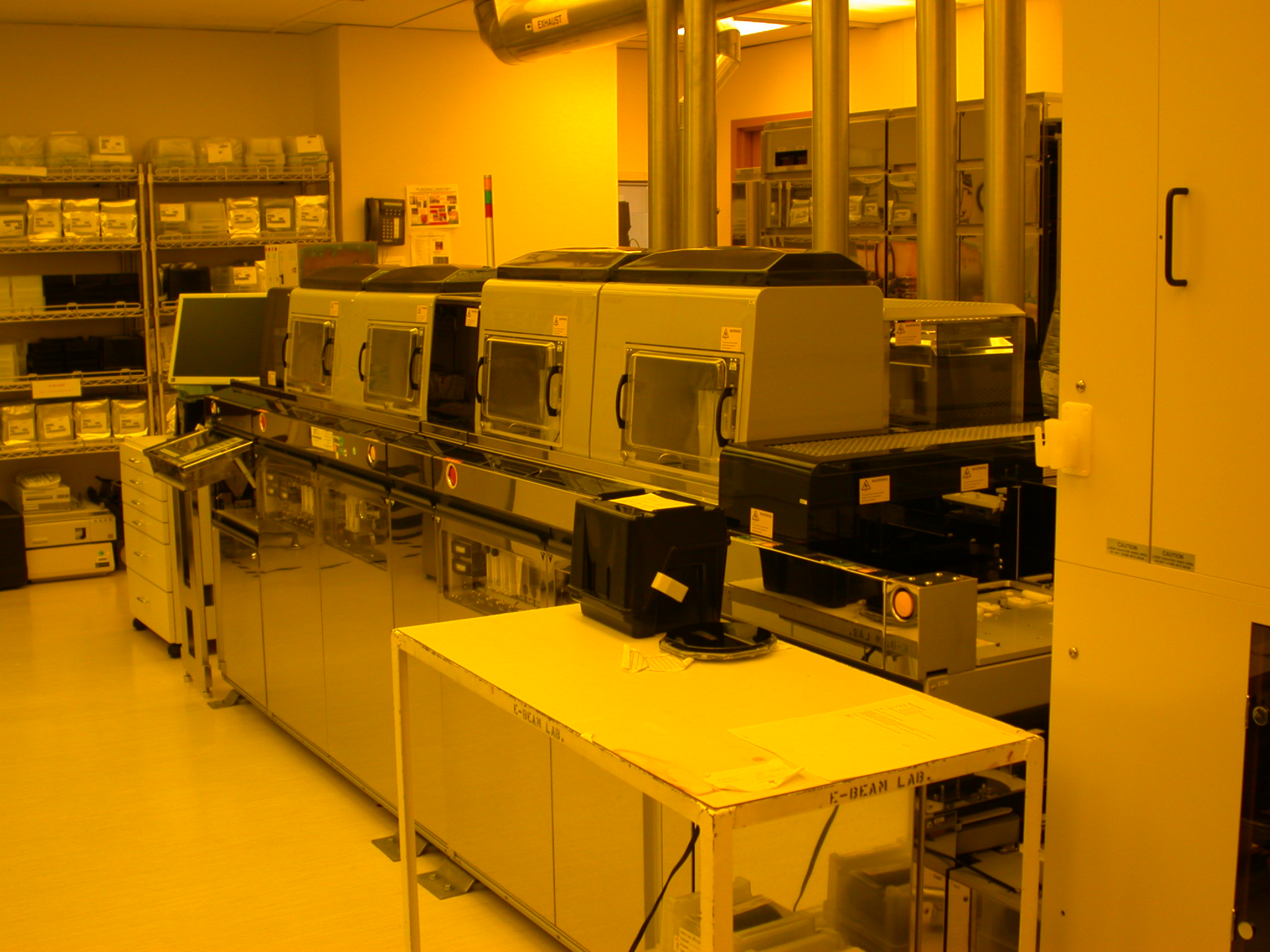
A process node isn't a single, precisely defined physical dimension but rather a generation of manufacturing technology. It broadly correlates with the minimum feature size, often the gate length or half-pitch of critical lithographic patterns, on a transistor. As nodes shrink, manufacturers can pack more transistors onto a single silicon wafer, leading to higher integrated circuit densities. This miniaturization is achieved through increasingly sophisticated techniques like Extreme Ultraviolet (EUV) lithography, advanced etching processes, and novel transistor architectures such as FinFETs and Gate-All-Around (GAA) transistors. The specific nm value is often a marketing designation, with different foundries using different metrics for their node naming conventions, leading to confusion but also highlighting generational leaps in capability.
📊 Key Facts & Numbers
The smallest commercially available process nodes have shrunk dramatically over the decades. A single silicon wafer can yield hundreds or even thousands of individual chips, depending on their size, with advanced nodes allowing for more chips per wafer. The cost of developing and manufacturing at these leading-edge nodes is astronomical.
👥 Key People & Organizations
Key players in the process node race include TSMC, the world's largest contract chip manufacturer, which produces chips for companies like Apple, Nvidia, and Qualcomm. Intel, historically a leader in integrated device manufacturing, is aggressively pursuing its foundry strategy with nodes like 20A and 18A. Samsung Electronics is another major integrated device manufacturer and foundry service provider, competing at the leading edge. ASML Holding is a critical enabler, holding a near-monopoly on the EUV lithography machines essential for sub-10nm nodes. IBM has also been instrumental in developing advanced transistor architectures, including early GAA concepts.
🌍 Cultural Impact & Influence
Process nodes are the invisible engines of the digital revolution, dictating the capabilities of consumer electronics, computing infrastructure, and emerging technologies. The relentless march of miniaturization, often dubbed Moore's Law, has fueled the exponential growth in computing power that underpins modern society. From the smartphones that have become ubiquitous to the artificial intelligence models that are transforming industries, the ability to pack more processing power into smaller, more efficient packages is directly attributable to advancements in process nodes. This has democratized access to powerful computing, enabling new forms of communication, entertainment, and scientific discovery, while also creating a global dependency on a highly specialized manufacturing ecosystem.
⚡ Current State & Latest Developments
The leading edge of process node technology is currently focused on 2nm and sub-2nm nodes. Samsung Electronics is also pushing forward with its 2nm GAA technology. Beyond these, research is ongoing into 1.4nm and even smaller nodes. A significant development is the increasing reliance on Gate-All-Around (GAA) architectures, moving beyond the FinFET design that dominated previous generations. Furthermore, the industry is exploring new materials and manufacturing techniques, such as cobalt and ruthenium in interconnects, to overcome the physical limitations of silicon scaling.
🤔 Controversies & Debates
The naming conventions for process nodes are a significant point of contention. The 'nm' designation has become increasingly decoupled from actual physical dimensions, leading to accusations of 'node stretching' where a manufacturer might label a process as '3nm' when its critical dimensions are closer to older '7nm' or '5nm' nodes. This makes direct comparisons between foundries difficult and fuels marketing wars. Another controversy surrounds the immense cost and complexity of developing new nodes, leading to consolidation in the foundry market and raising concerns about accessibility for smaller chip designers. The environmental impact of semiconductor manufacturing, including high energy and water consumption, is also a growing concern, particularly with the increasing scale of fabrication plants.
🔮 Future Outlook & Predictions
The future of process nodes points towards continued, albeit slower, miniaturization. While the traditional scaling of silicon may be approaching fundamental physical limits, innovation is shifting towards new transistor architectures like GAA, advanced packaging techniques (e.g., chiplets), and novel materials. Companies like IBM and imec are researching beyond 1nm, exploring concepts like vertical transistors and new semiconductor materials. The focus is also broadening beyond raw transistor density to include specialized architectures for AI and quantum computing. The industry anticipates a potential slowdown in the historical pace of Moore's Law, necessitating a greater emphasis on architectural innovation and system-level optimization to continue performance gains.
💡 Practical Applications
Process nodes are the bedrock of virtually all modern electronic devices. High-performance CPUs and GPUs for personal computers and servers, the processors in smartphones, AI accelerators, 5G modems, and advanced automotive chips all rely on the capabilities enabled by specific process nodes. For example, a cutting-edge smartphone might use a 3nm or 4nm class processor for its main SoC, while a high-end gaming console GPU could be fabricated on a 5nm or 7nm node. Even specialized applications like medical imaging equipment and aerospace systems benefit from the increased power efficiency and performance offered by advanced nodes.
Key Facts
- Category
- technology
- Type
- topic